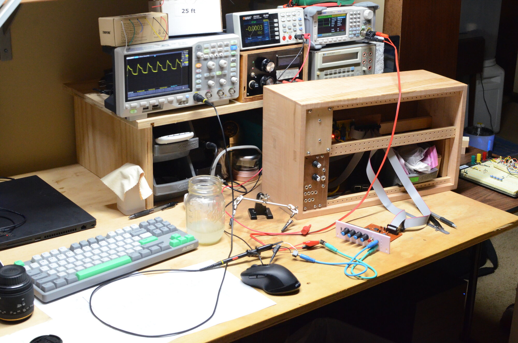
In the previous post, we looked at the process for making a double sided PCB for the front panel components of an analog sytntheziser module. Now we're going to look at the module itself.
WTF is an Envelope Generator?
Very briefly, An envelope defines the extremes of some signal over time. In electronic music, envelopes are used as inputs to modules like VCAs (voltage controlled amplifiers), and VCFs (voltage controlled filters. Read a more thorough explanation at sdiy wiki.
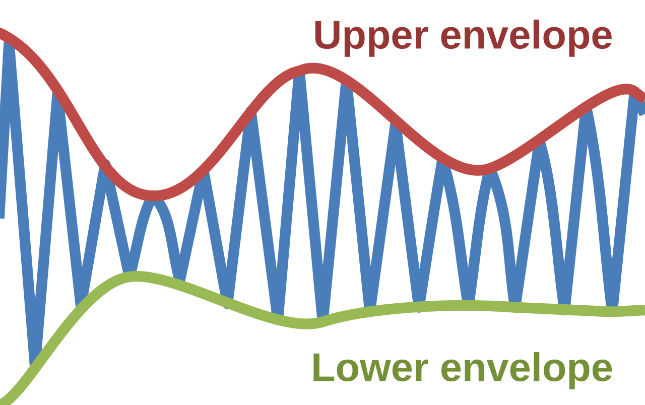 via Wikipedia
Design Detour
There are many existing designs for envelope generators. The simplist AR (attack/release) can be made with 2 potentiometers, 2 diodes, 1 capacitor, and some way to buffer the capacitor voltage (example article).
I originally tried to design an ADSR envelope generator circuit using switched currents into a storage capictor. The advantage versus the simpler voltage source through a resistor would be linear ramps of the envelope shapes instead of the exponential rise/decay, the ability to use input voltages from other sources, and removing the need for logaritmic potentiometers (assuming you use an exponential converter on the input voltages).
I ended up getting a little lost in the weeds with my design though, and never actually made a working circuit. From some archeological research into my own notes, it seems like I was trying to use discrete JFET analog switches for each input voltage, and a diode bridge current switch (which I still think is kinda cool). diode bridge circuit explaination video from w2aew on youtube
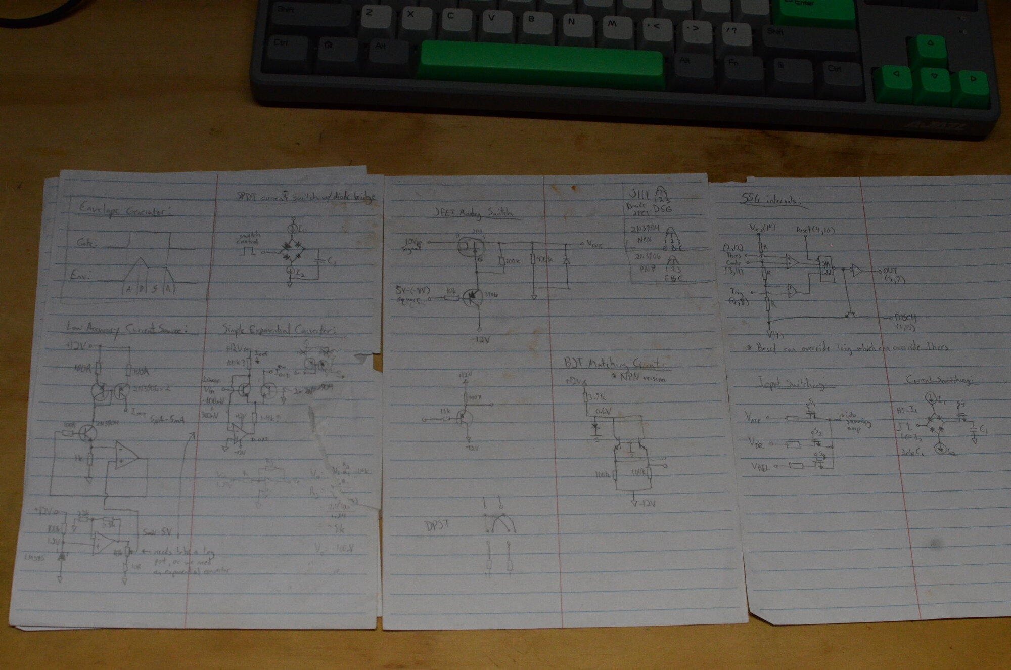 Interpreting hieroglyphics is as much an art as it is a science.
Using an Existing Design
At some point, I moved on to designing a VCA, and then came back to the envelope generator earlier this year. Determined not to get stuck again on weird designs, I looked for existing circuits that would be easy to build and test. I settled on a design by René Schmitz which uses a 555 timer, along with some extra diode logic to separate the storage capictor during the envelope phases.
I made a few minor changes to René's design by adding a manual trigger, and gate LED connection for the front panel. I also added a 5V connection to the 555's CV pin along with some extra diodes to clip the output to 0-5V. In hindsight, it would probably use the same number of added components to do scaling and level shifting at the output buffer op-amp.
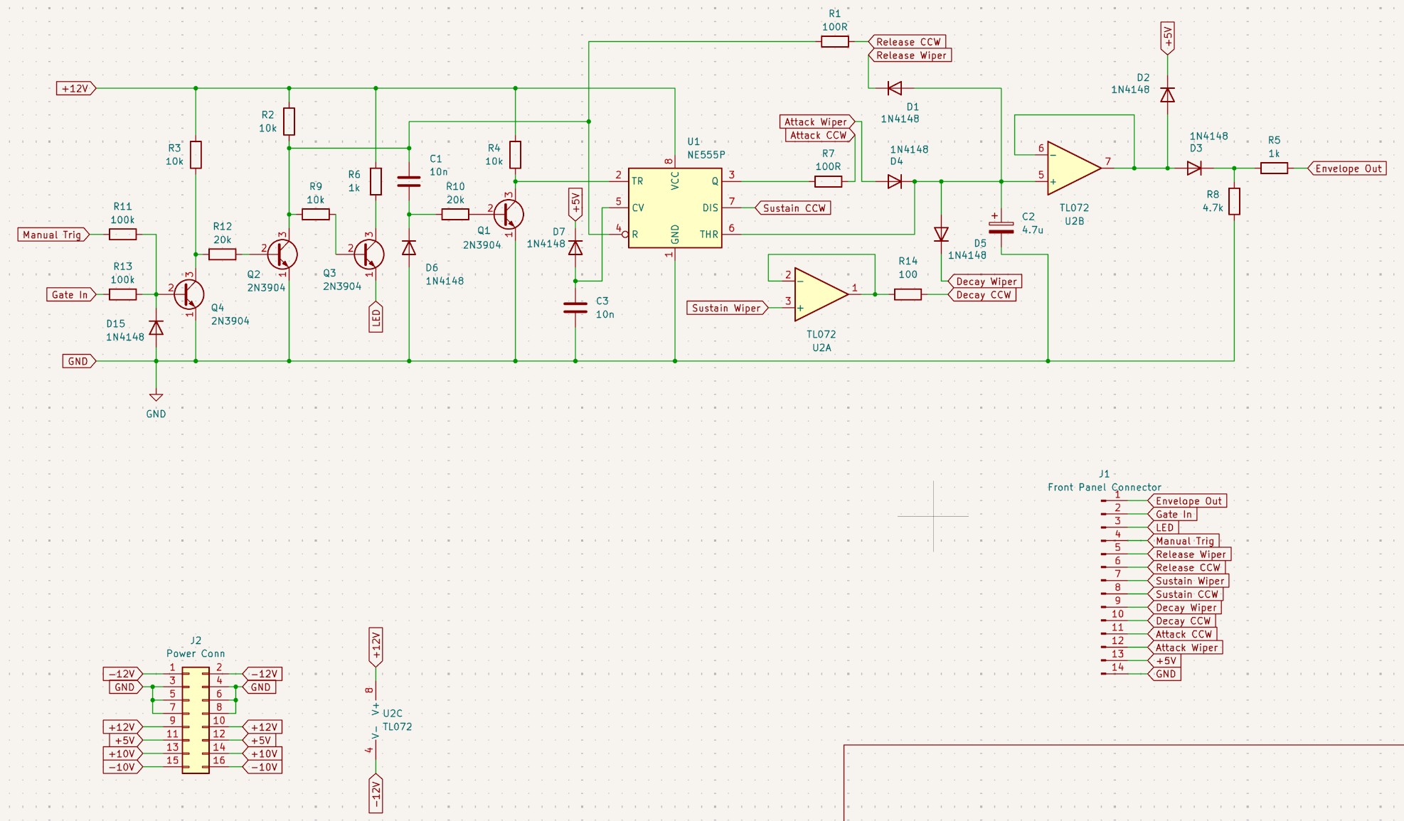
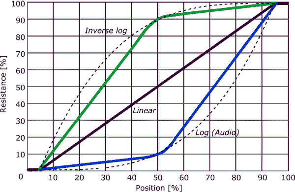
As mentioned earlier, the downside of this circuit, and others that use potentiometers to change the charging and discharging time constants, is that you don't get as much dynamic range from the inputs as a true exponential converter. This is mainly because (inexpensive) audio taper potentiometers are not really logarithmic, they are a manufacturing compromise that combines two or more tapered slope profiles to mimic a logatrithmic profile. This is most apparant at the extreme ends of the potentiometer travel, and limit the usable range of the circuit at different music tempos depending on the choice of time constant.
For a revision two of this circuit, a useful addition would be a switch on the front panel to switch in 2 or three capacitors for slow, medium, and fast tempos.

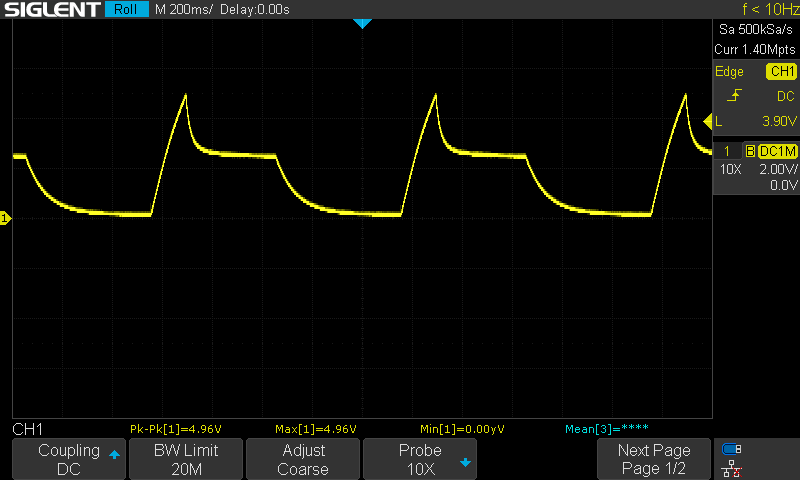 A better view of the exponential decay from the linear RC circuit.
Construction Notes
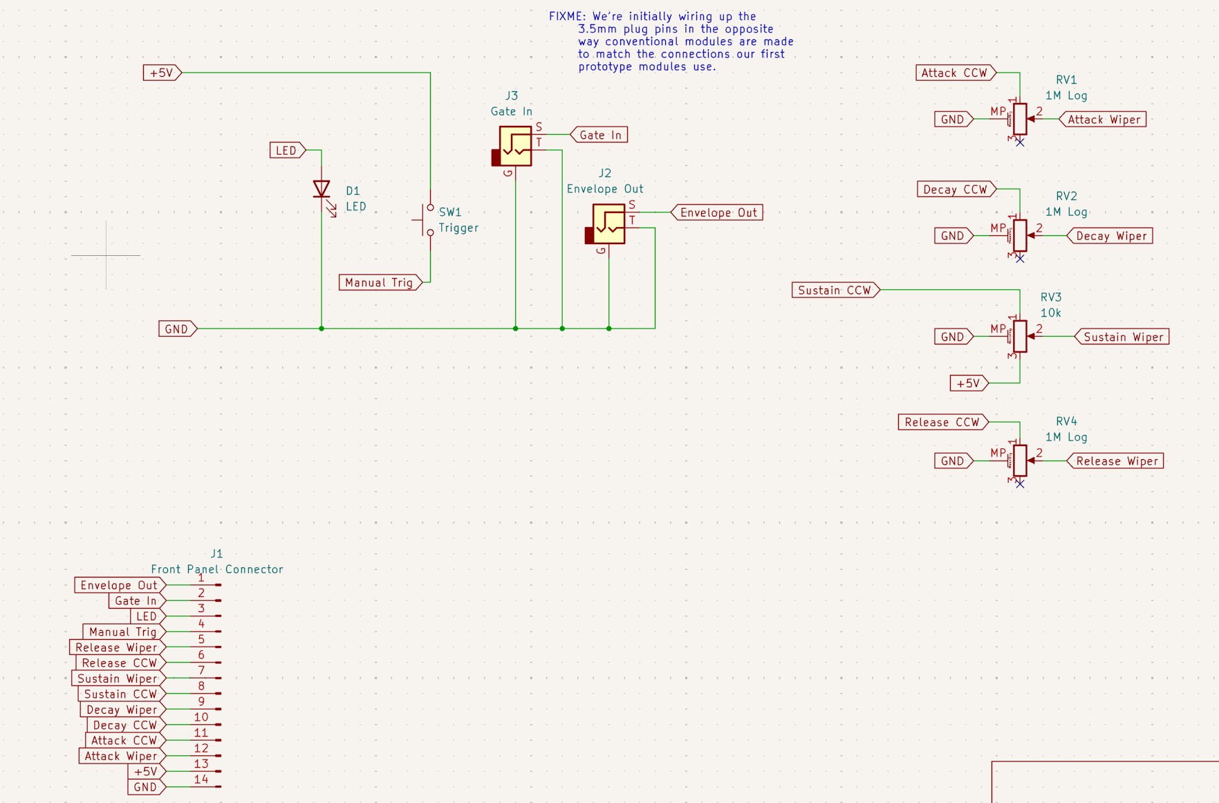
As I noted in the front panel schematic, the mono jack connections are wired to use opposite pinouts compared to exising audio equipment conventions. It's one of those situations where there's an arbitrary choice that is only important to be consistant. I'll need to remember to update my design before starting on a filter module panel, and to add front panel PCB layouts to the other existing designs.
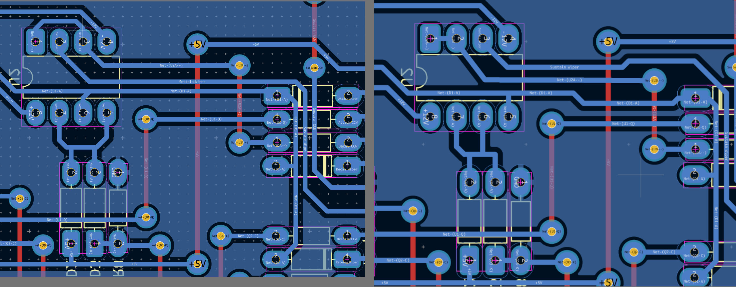
When doing the schematic capture from the breadboarded circuit, I made the mistake of not flipping the op-amp symbols to match the non-inverting configuration. I've made the same mistake before, but I think this is the first time it made it all the way into the PCB.
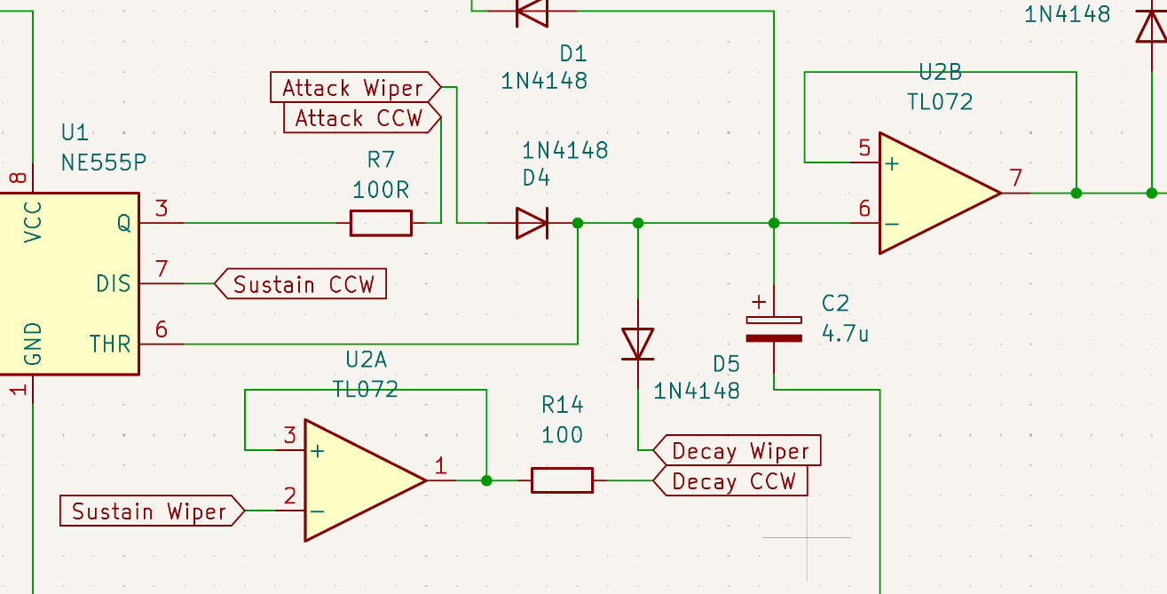
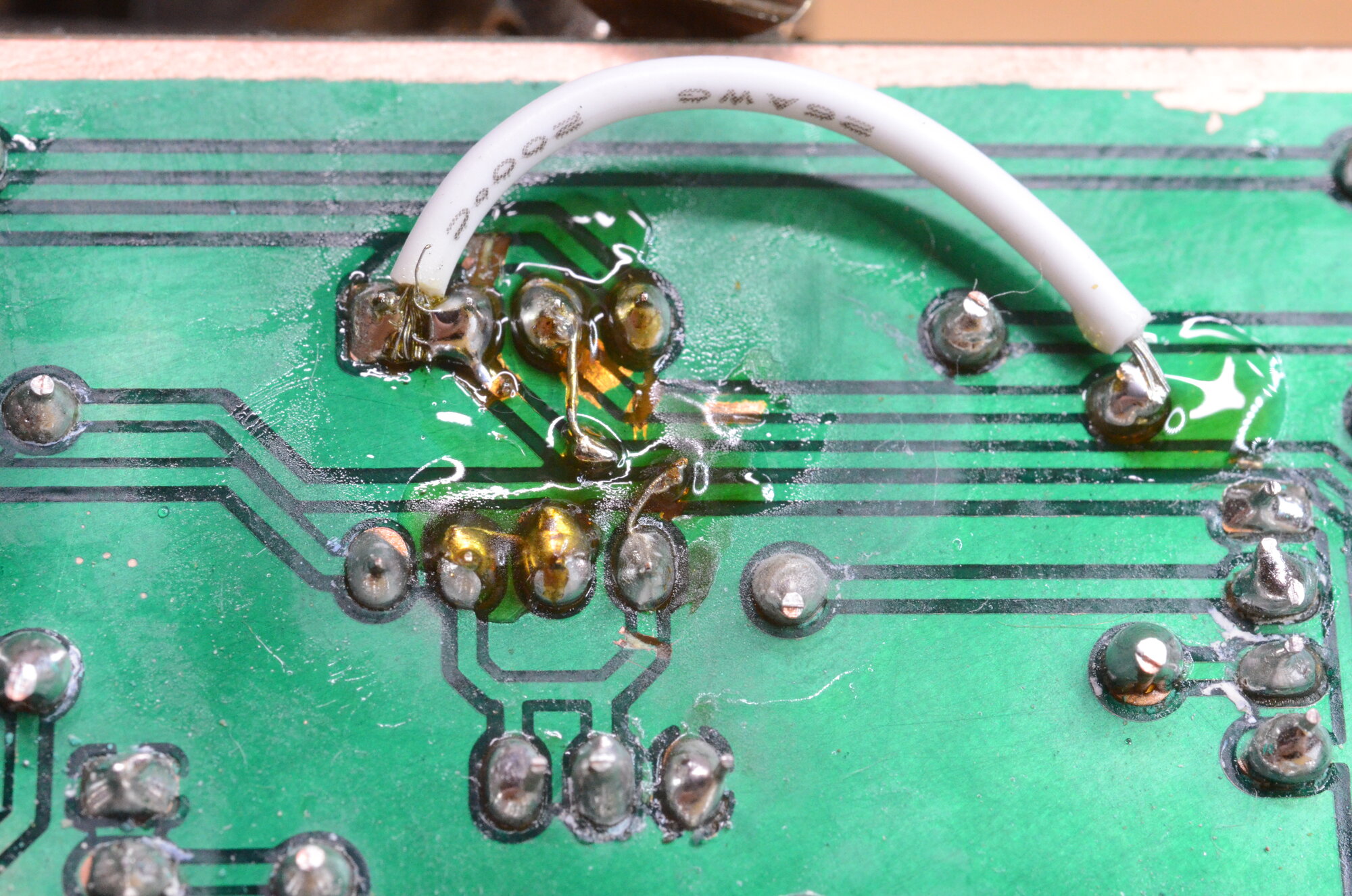
I made sure to correct both the schematic, and the PCB after confirming that the circuit worked properly after some nice bodging.
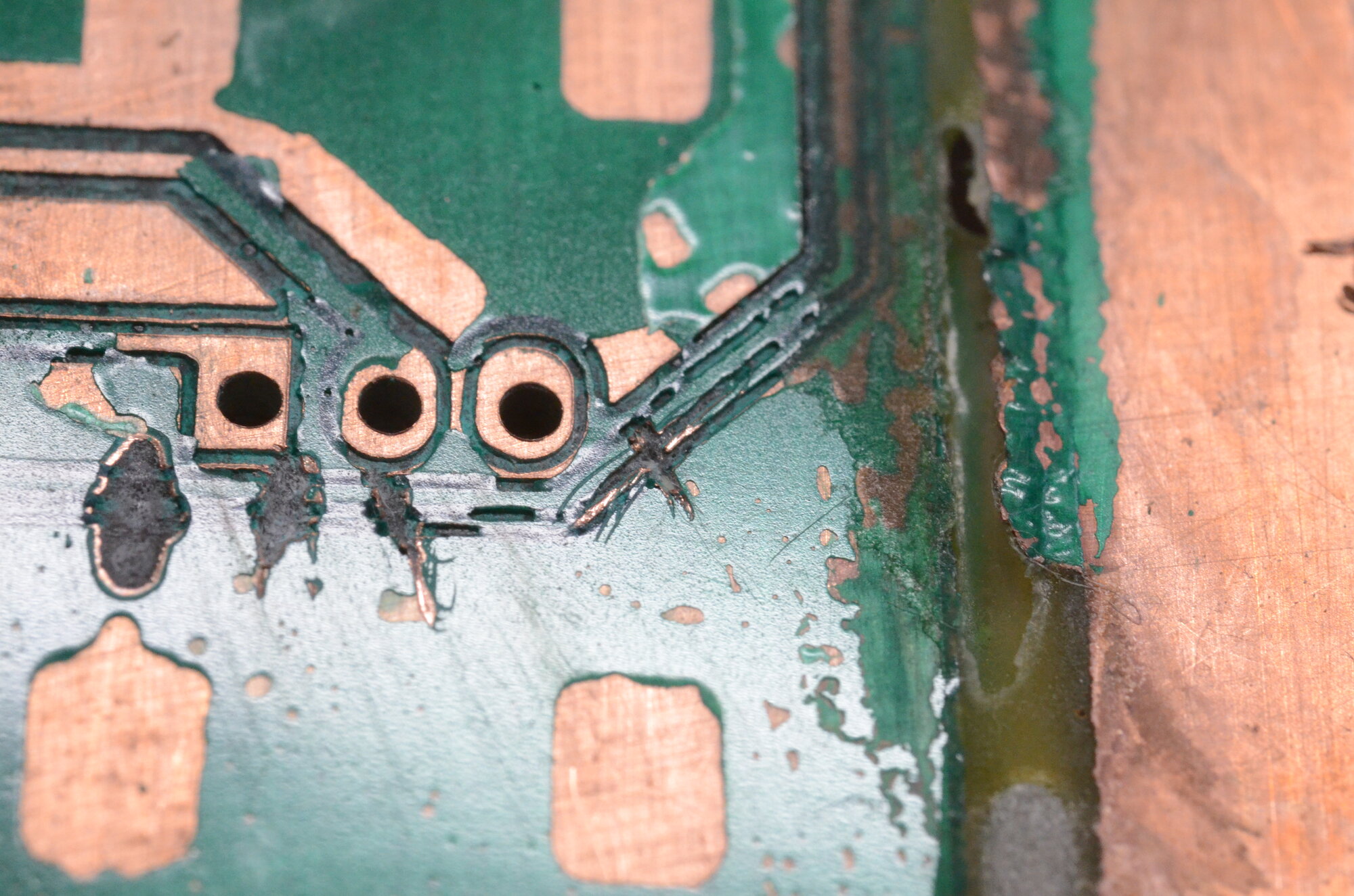
I also did a little test to see if I could do any better than a sharp exacto blade by hand (right) with a dremel with different tips (left 3) to cut the PCB traces. Seems like the hand tool wins.
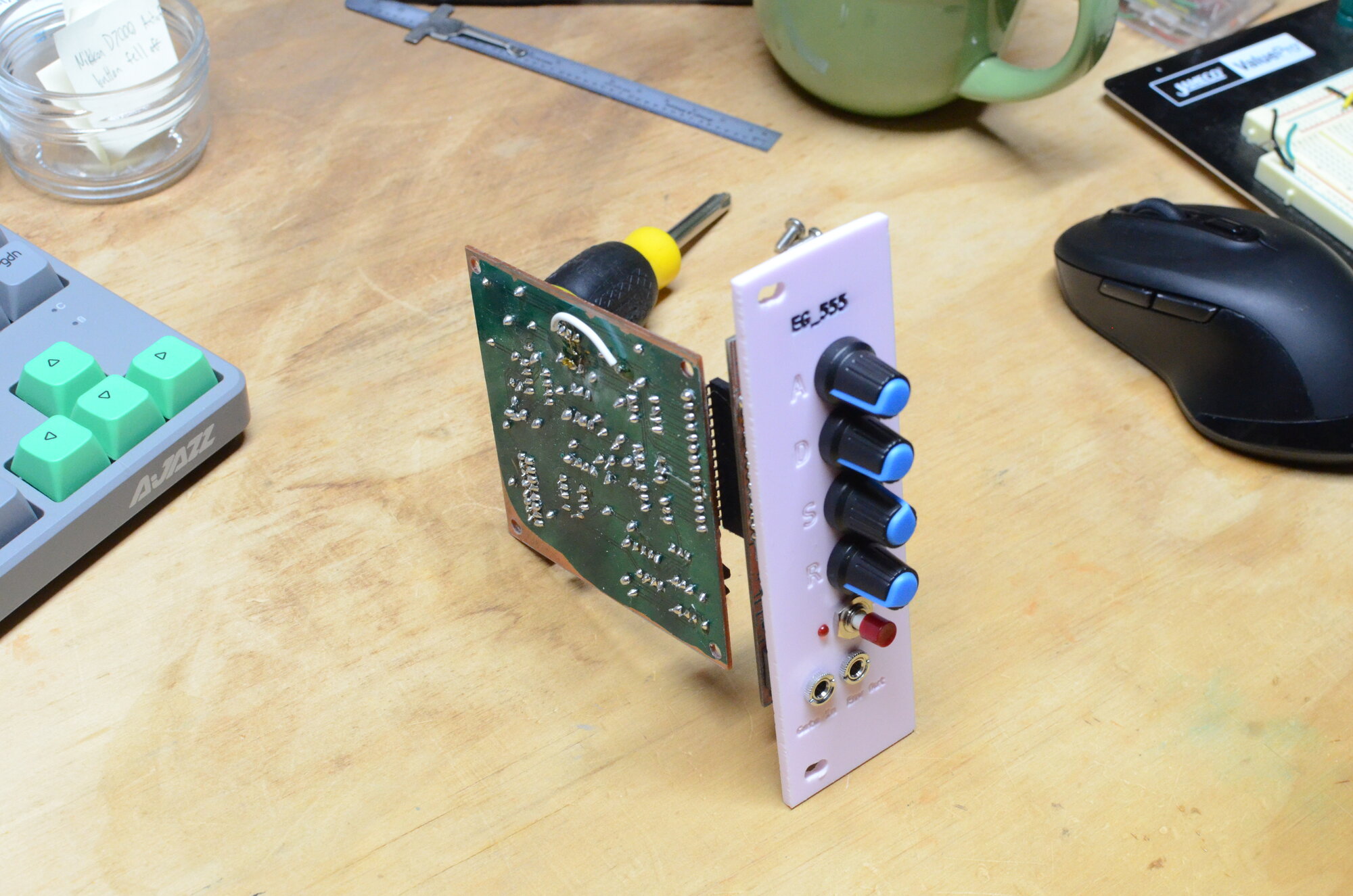
My final change was to move the front panel connector to the very edge of the board. It uses a 90 degree 2.54mm pin header to connect to the front panel, and wouldn't quite plug all the into a breadboard when testing the original design. Some extra glamour shots of the assembled module:
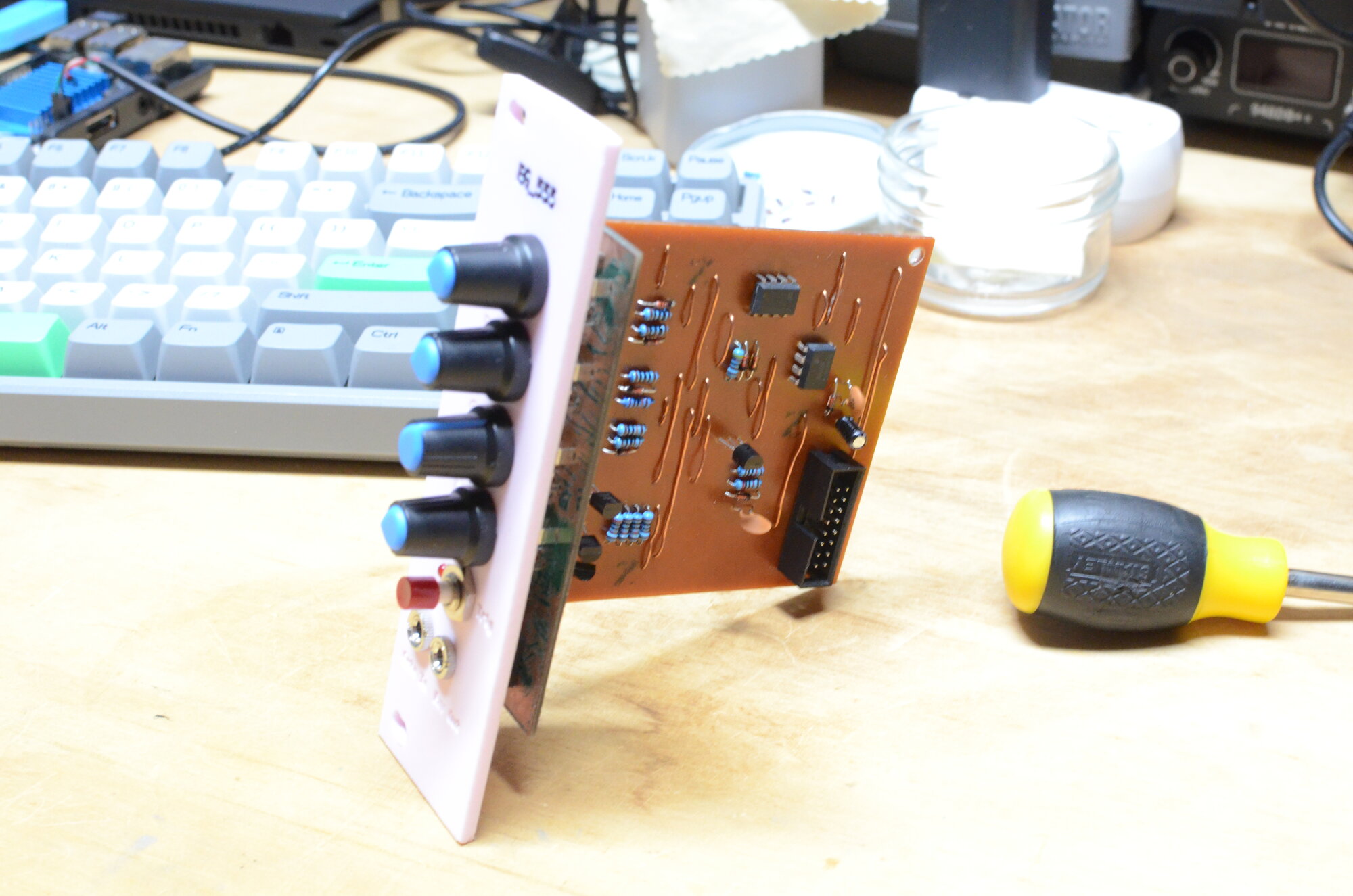
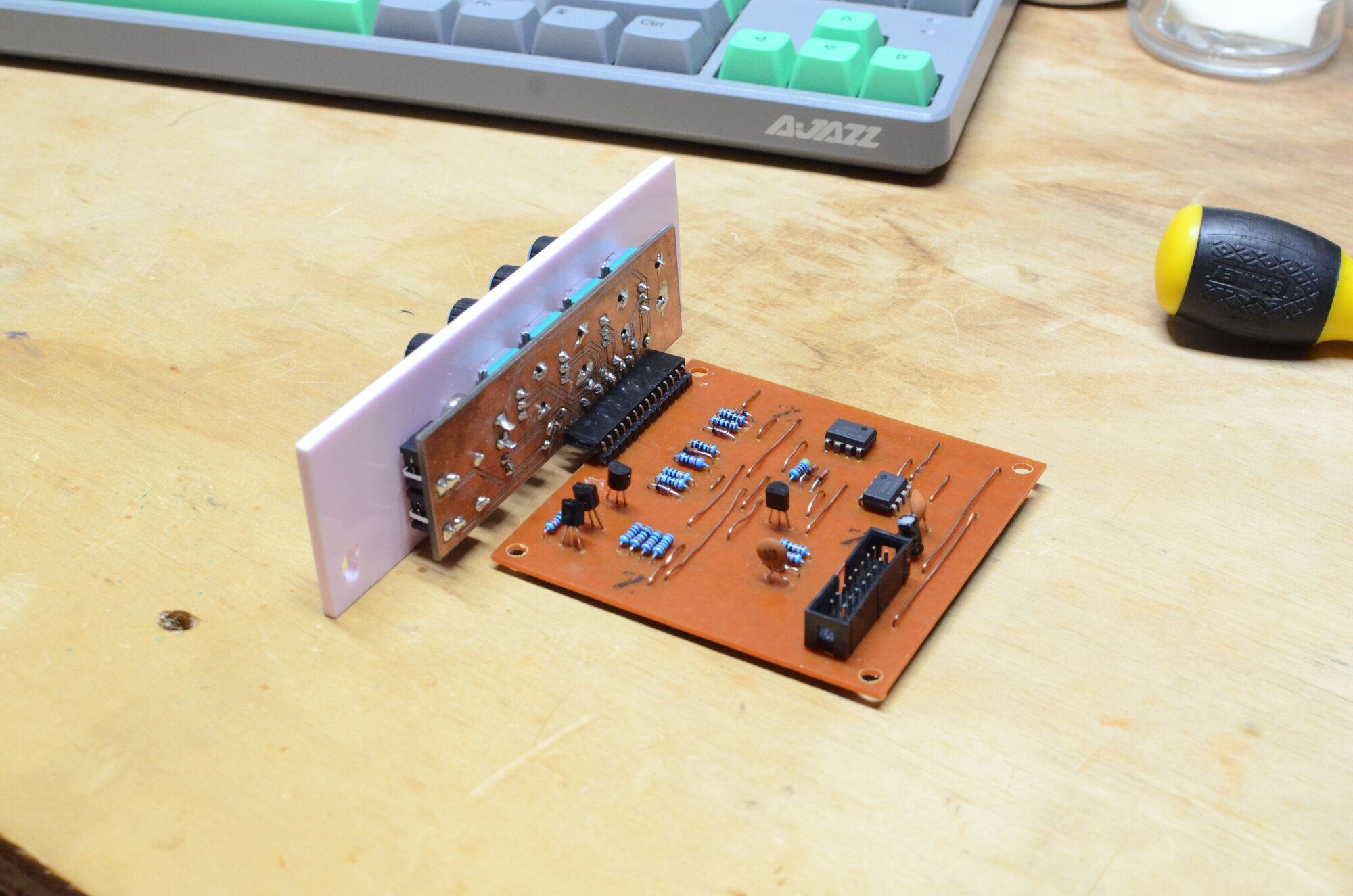
Hopefully in the next post I can talk about designing, and milling the acrylic front panel, but I still have more testing/learning to do with FreeCAD. I would also like to add some brackets from the acrylic panel to the main board for better support, and try to reduce the front panel width by another 1/2", which is the mounting hole spacing for my case.