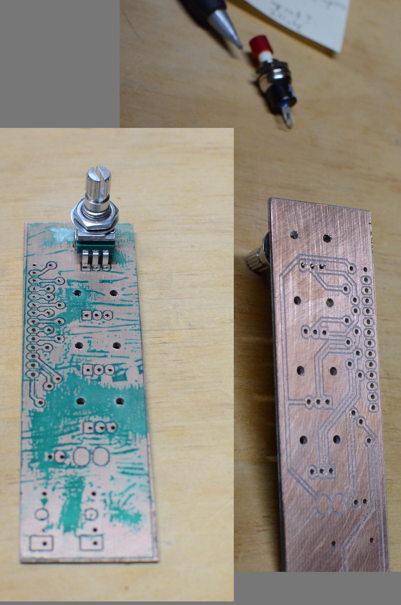
Intro
I've been wanting to try milling double-sided PCBs for awhile, and I finally have a good reason. I'm trying to make an easier to assemble front plate for an analog synth module. Previously, I have been making connections to jacks and potentiometeters with soldered wires that terminate in connectors. This works ok, but it's hard to tell which wire is going to which pin on the busier front panels. This is especially bad when using a ribbon connector because most of the wires are the same color.
I've seen that a lot of the commercial modules use a stacked board setup where the front panel components have one PCB that is then connected with pin headers and spacers to other boards all in the same orientation.
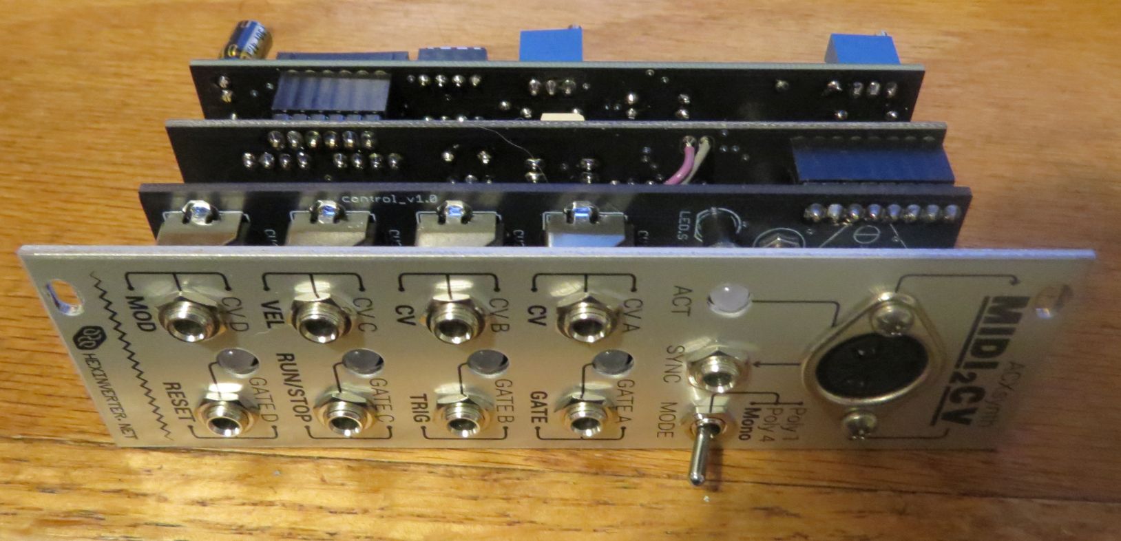 image found at: https://www.djerickson.com/synth/
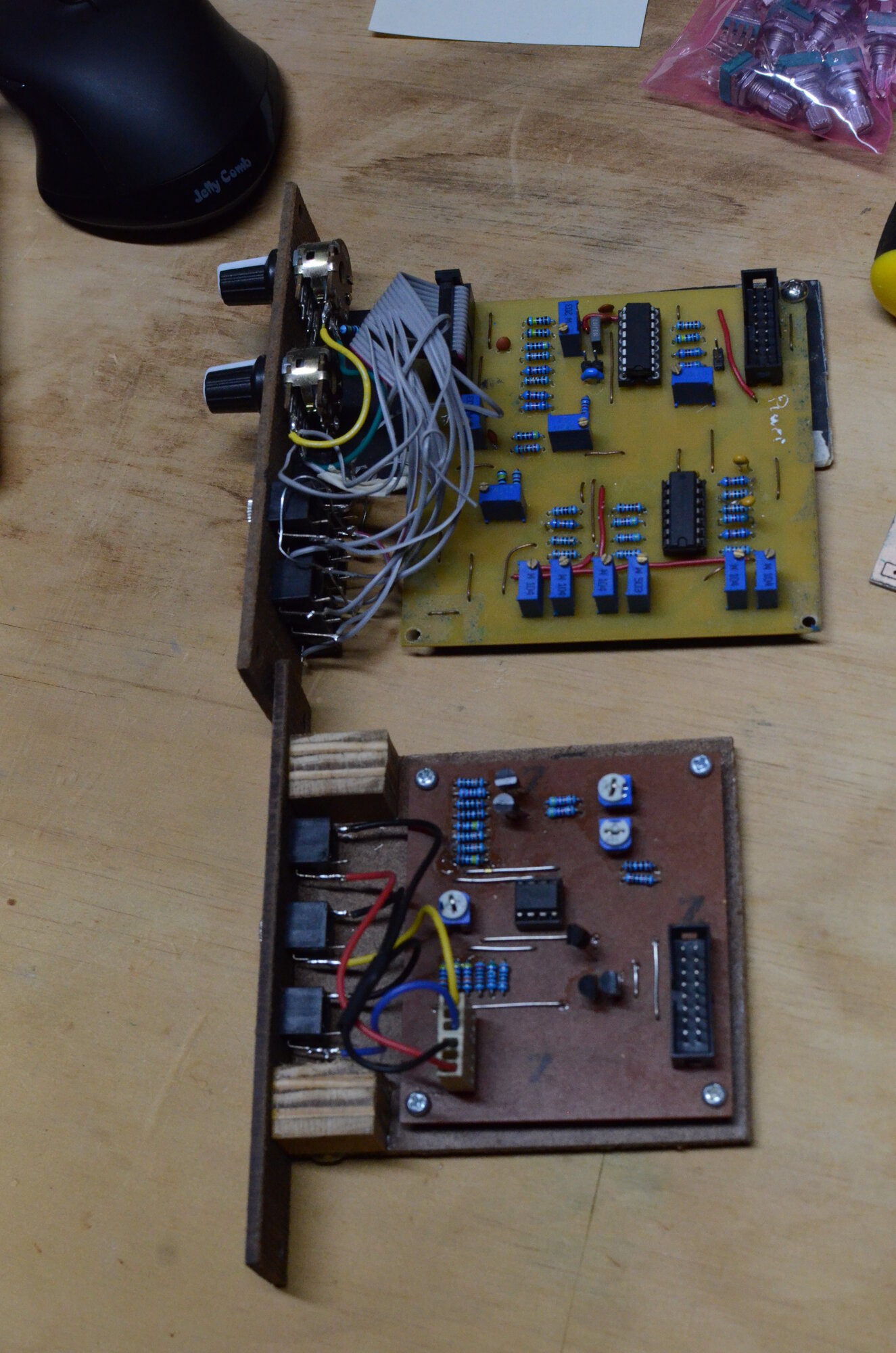
With my own modules, I've been using a construction similar to a "Eurocard", with the PCB mounted perpendicularly to the faceplate. At least with homemade PCBs, you have more room to work with as long as your rack is deep enough. In my case, I have around 140mm of usable depth for the modules, which works out well for 150mmx100mm blank PCBs.
Either design presents a problem for single-sided PCBs. You have the panel components that need to be soldered on the 'back' side, and a connector that needs to be soldered from the 'front' side then routed back to the other side of the board where all your traces are. So, now I have an excuse to get double sided milling working.
Setup:
I'm using one of the cheapest CNC milling machines you can buy that still has limit switches: link. I found one used on ebay for $160 a few years ago after getting starting in hobby electronics. For engraving at -0.1mm, and drilling 1mm through holes, it works really well. Where it struggles the most is when cutting out a board or making pockets in wood. I recently tried a very gentle 50mm/min feed rate at 0.5mm depth passes for a 2mm end mill, and the vibrations and noise were just as bad as milling at 150mm/min and 1mm depth. I think this is an indication that the frame is just not stiff enough for any sort of lateral load. Still, if you can put up with a hideous noise for around 5-10 minutes, it will power through. Otherwise, I would recommend looking for something a little larger and more expensive.
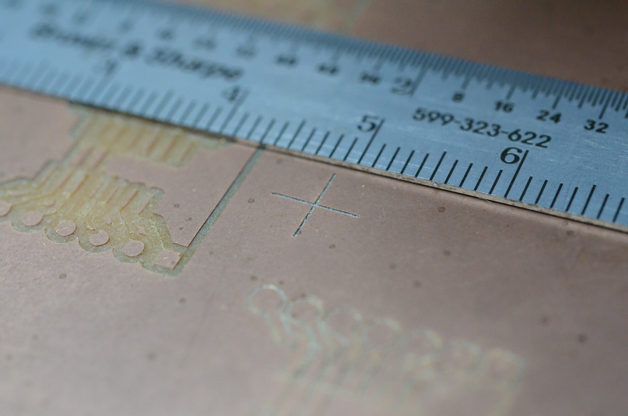
Unsuprisingly, you need a way to align the front side of your PCB with the back side to connect the traces properly. I'm using a point in machine coordinates that can be reliably returned to after an alarm or software reset. The image below shows an engraving of the same shape after resetting, then re-homing the machine, and re-probing for the z coordinate:
To reliably get a board in this location, I'm using 2 dowel pins just below the Y axis as a stop, and 2 more pins 50mm above that will go directly into the board:
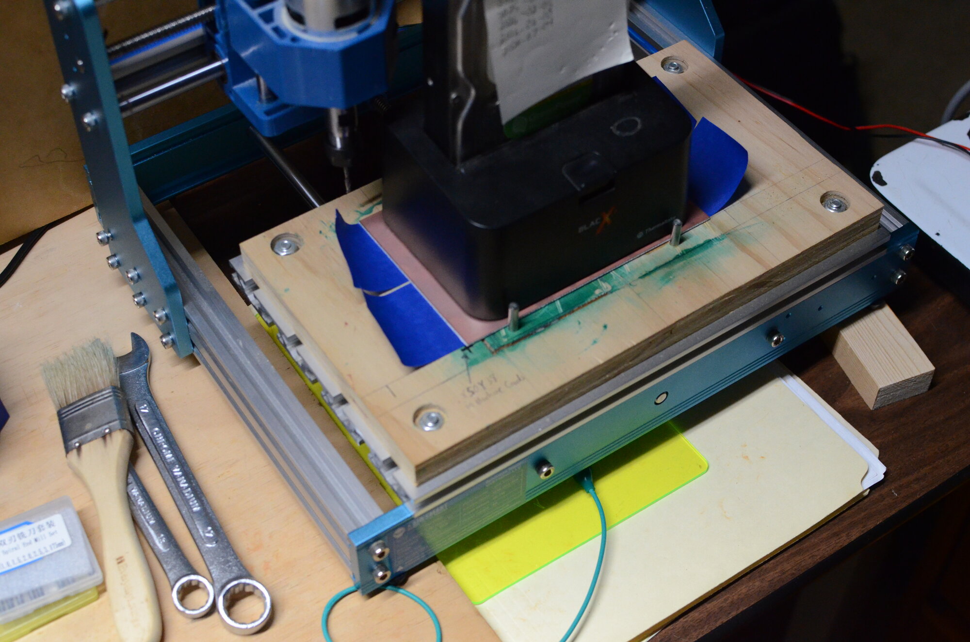
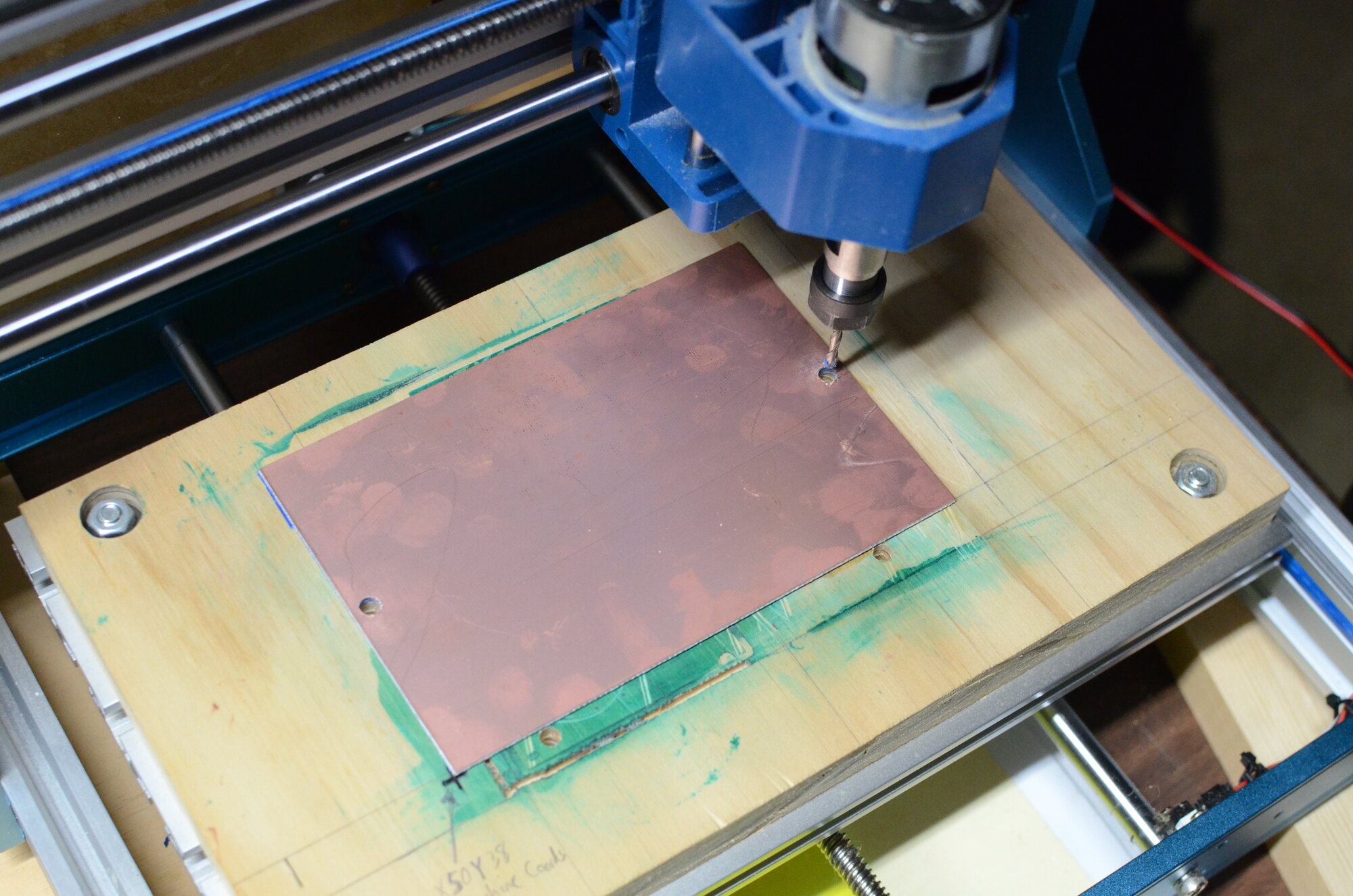
The 2 pins that go into the board set your axis of rotation when flipping the board over. Now when generating your g-code for the machine, you can use a y-axis at 50mm as a mirror axis.
Software:
Your choice of software will largely depend on where you start, and where you end. In my case, I start with a KiCAD PCB design, and need to send the g-code to a GRBL CNC controller. (See the warning on the linked wiki page about GRBL, and consider using a newer firmware if you are looking for a new machine.) I also prefer to use software that I can run natively on my linux computers, which is a little limiting, as there are a lot of tools that are made for Windows. With a little experimenting, I've ended up with the following:
| Role: | Tool: |
|---|---|
| EDA | KiCAD |
| g-code generator | pcb2gcode and GUI |
| g-code sender | bCNC |
For the g-code sending software, I have had much better results when probing a heightmap grid before the engraving step. Even if it was possible to mill a perfectly flat spoilboard on the CNC, I have measured 0.05mm deviations in the blank PCBs I use. That plus the variability of the 2 layers of painters tape with superglue in between for workholding means that an engraving depth of 0.1mm is hard to achieve without some extra help.
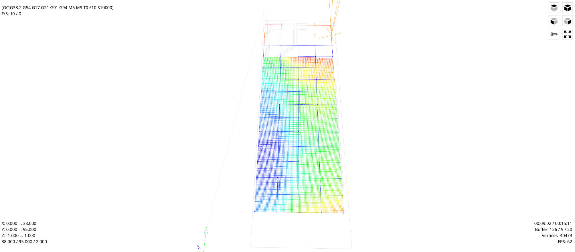
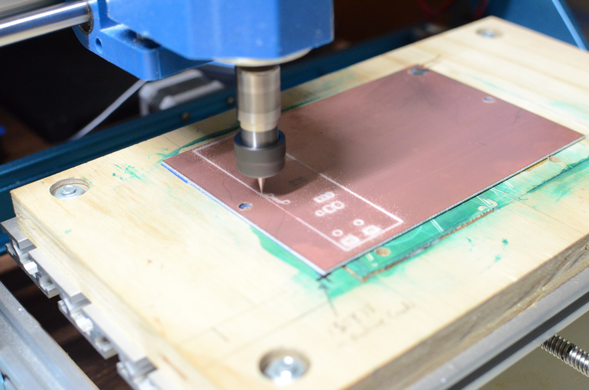
I had previously used a fork of Candle, Candle2, as a g-code sender, but got frustrated with it constantly resetting my work coordinates even when not responding to an alarm. For some reason, Candle2 also insisted on starting a heightmap probe by probing at 0,0 in work coordinates, which is right on the edge of the PCB. I switched to bCNC when I saw that it would probe only in the area you specify, along with some other useful built-in tools like a 'scan' function that will move the CNC in a rectangle around your toolpaths to easily see if your workpiece is positioned properly. Most importantly, bCNC does not reset your work coordinates when you stop an operation in progress! It even gives you a warning dialog that recommends you to re-home your machine after an alarm.
Another option for the g-code generator stage is FlatCAM, which seems to have been popular in the past, but is now difficult to install on a current linux distribution because of the python2 dependancies.
I think that no matter what combination of software you choose, it will require some experimentation to learn, and find settings that will work with your setup. Be prepared to ruin a lot of blank PCBs, and break many bits. It turns out they are called 'consumables' for a reason.
If you want to start with the same setup I'm using, or are me in the future, I will put a repo with FreeCAD files for the alignment pins, and pcb2gcodeGUI settings: link
Other Notes:
You may have noticed in the 'success' image at the beginning that the UV curing solder mask didn't turn out very well. The solder mask isn't strictly a requirement, but it does help with preventing solder bridges when assembling the components onto the board. I've used this ink successfully before in the same conditions, with the same calibrated UV light and curing times.
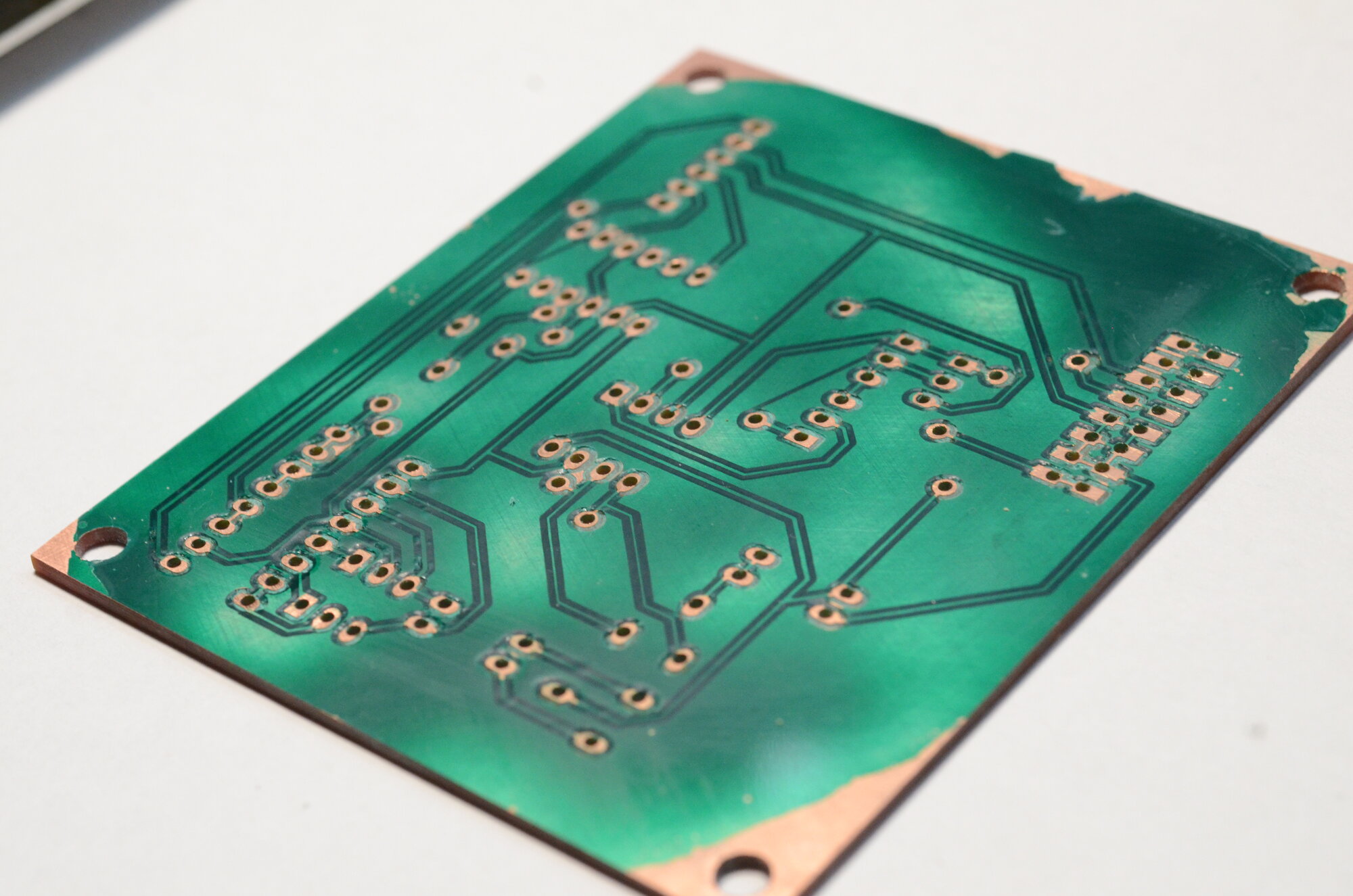
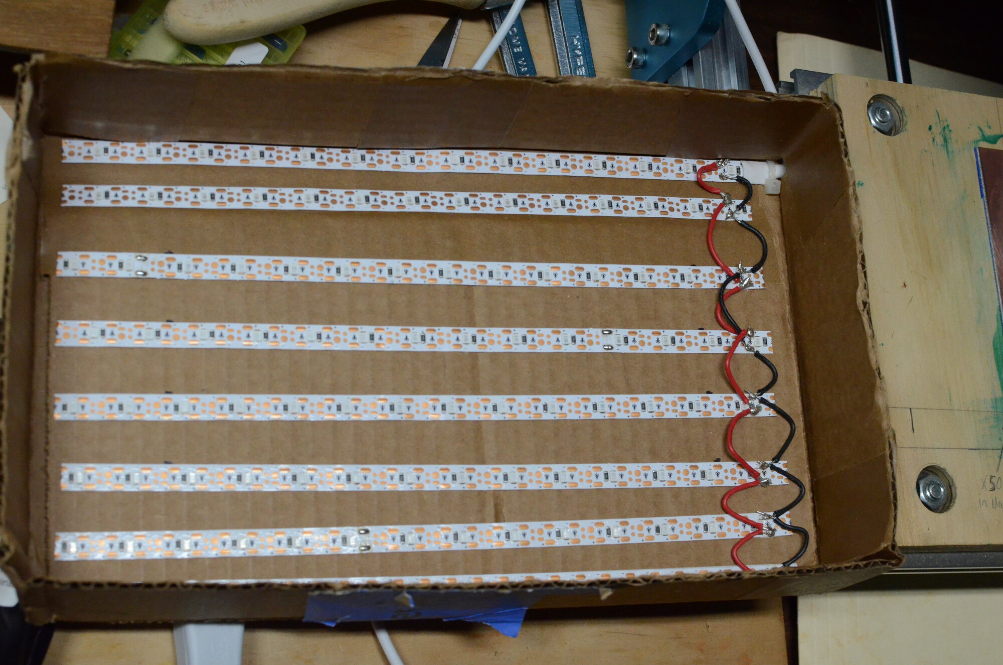
My surface prep is to clean and rough up the copper with a scouring pad, then wipe clean with 90% isopropyl alcohol. I use 2 layers of transparency film with the soldermask pattern from a laser printer placed over the board with a sacrificial sheet directly on the ink. In about 10 minutes, the ink will set enough to wipe off the pads with some IPA on a paper towel. Then fully cure for another 15 minutes.
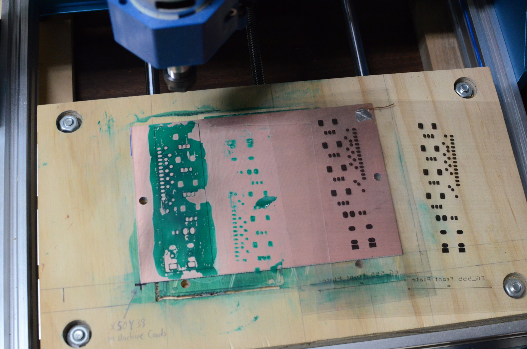
It's hard to find reliable information from a search engine in the age of AI slop, but it seems that the ink itself could be starting to deteriorate. I double-checked with my bench agent who concurs:
 Indubitably
Update 2026-07-31:
I have two corrections to make from the article:
It turns out, the UV ink works just fine, but I hadn't spread it out thin enough. I had this figured out, but since it had been awhile since I last made a board, I forgot why using a paintbrush doesn't work. Maybe with a different paint, or stronger UV light, it might not matter, but what does work is cleaning the pcb, applying some ink, then adding the sacrificial piece of transparent printer film. Then, carefully spread the ink out by applying pressure from the top of the film with a straight edge (even a credit card works for this, it just needs to have some flex). The idea is the squeeze the ink into a very thin layer, which is one more thing that takes some practice. Here are some pictures of the end result of the main board I made recently after re-learning how to apply the ink:
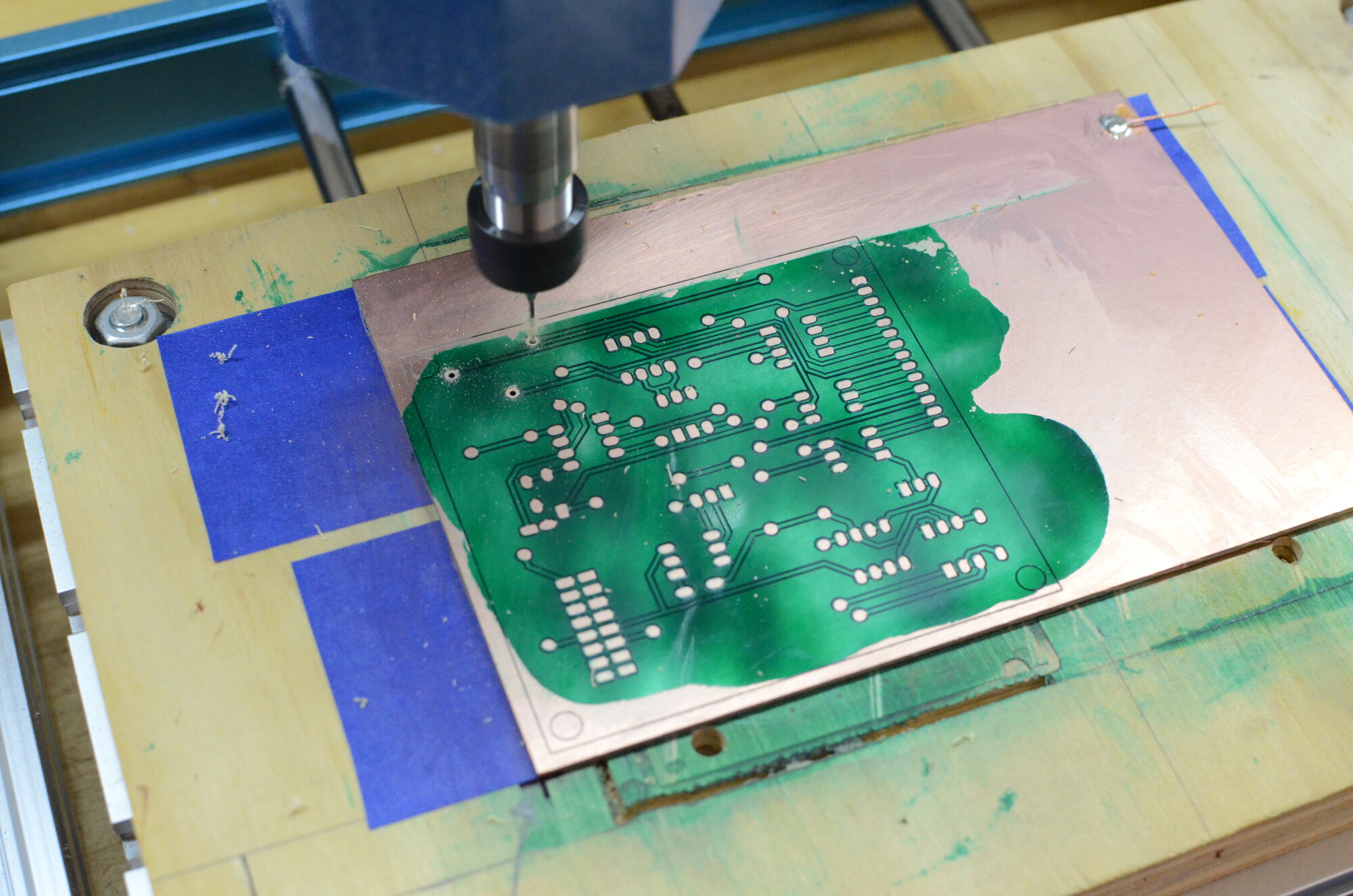
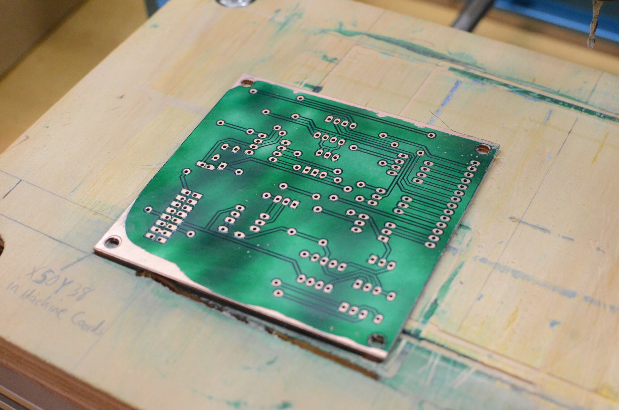
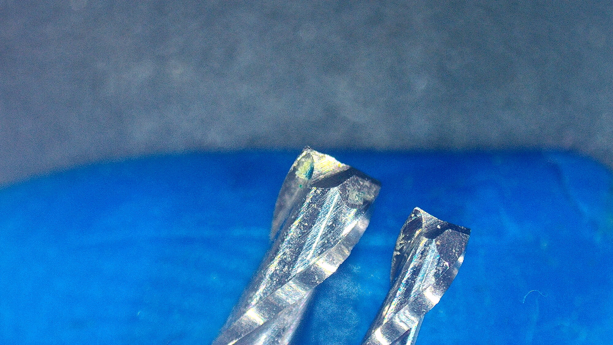
Second, The vibration and noise from cutting the PCB out seemed worse than I remembered, and I think that was due to a worn end mill bit. I've been re-using the same 2mm end mill bit for awhile, since it's the only one in that size I have left, and all my gcode expects it. For milling single sided boards, I found some blank phenolic boards that seem to be pretty easy on tools. The double sided blank boards are FR4, made on a fiberglass substrate, and is apparently a much more abrasive material for the tools. I think the recommendation for using a bigger CNC machine for milling is still applicable, but I'll order some new bits, and test again before I look at upgrading. Here's a microscope image showing the difference between the old bit and a fresh one: